Summary: What Conductive Filament Can and Cannot Do
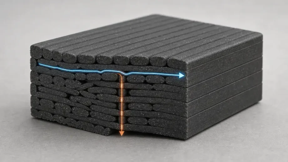
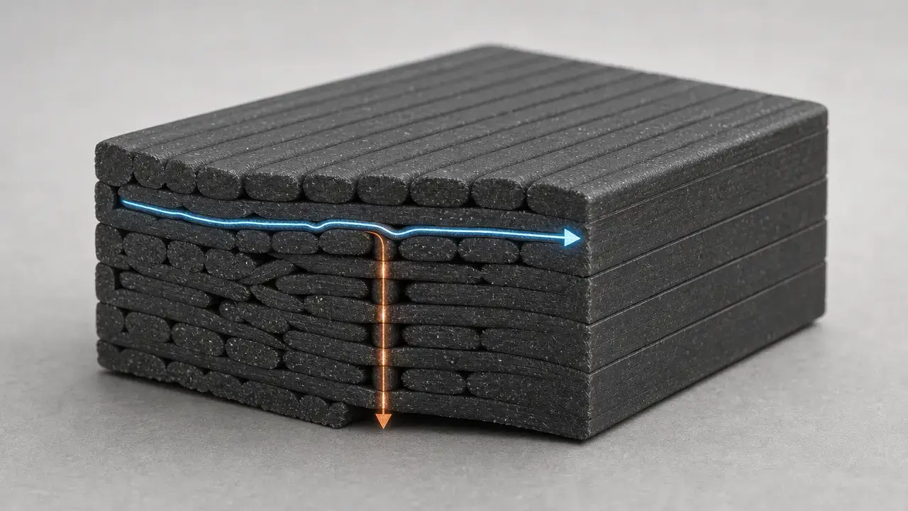
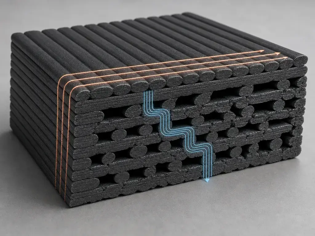
Conductive filament can make printed parts that bleed off charge, sense touch, or carry small currents, but its usefulness depends on designed-in resistance and measured geometry, not on a simple yes-or-no “does it conduct” test. ProtoPasta, for example, reports conductive PLA at 30 Ω·cm in printed XY parts and 115 Ω·cm through Z on its technical page, showing how strongly print direction can matter. [8]
For ESD work, the important numbers are resistance windows, not wire-like conductivity. ESDA defines conductive materials as having surface or volume resistance below 1.0 × 10^4 Ω, dissipative materials from 1.0 × 10^4 Ω to below 1.0 × 10^11 Ω, and insulative materials at or above 1.0 × 10^11 Ω. [4] That makes ESD-safe filament a different target from a low-resistance circuit trace. Meter readings can also mislead because the contacts may contribute resistance of the same order as the sample: Multi3D gives a manufacturer example of 0.5 Ω with silver paste and 2.4 Ω with screw terminals. [11] Independent printed-trace data show an even bigger spread by filler family, with 12 Ω·cm for carbon black, 0.78 Ω·cm for graphene, and 0.014 Ω·cm for copper-filled filament in one peer-reviewed study. [17]
What Conductive Filament Is
Conductive filament is an electrically conductive or charge-dissipative feedstock for additive manufacturing. In practice, that usually means a thermoplastic loaded with conductive filler so a printed part can pass current to some degree, leak charge, or change resistance under touch, strain, or contact. ISO/ASTM 52900:2021 is the vocabulary anchor for additive manufacturing terminology, and related ISO/ASTM material-extrusion documents use material extrusion for the plastic-process family discussed here. [1] [27]
Many readers still search for FDM and FFF, so those terms remain common in user-facing writing. This article uses material extrusion as the broader process label, because conductive behavior depends on extrusion paths, interlayer bonding, voids, and the direction current must take through the printed structure. [1] [27]
Common conductive filler families:
- Carbon black
- Carbon nanotubes
- Graphene or graphitic carbon
- Metal-filled or metal-polymer systems
- Flexible conductive elastomers
Graphene and graphite should not be treated as interchangeable scientific terms. IUPAC distinguishes graphite as a three-dimensional stacked structure and reserves graphene for the single-layer case or single-layer-derived discussion. [23]
The Numbers That Matter: Resistance vs Resistivity vs Conductivity
Resistance is the opposition of one specific printed part, trace, or coupon to current flow, so its unit is ohms (Ω). Resistivity is the material property behind that behavior, which is why volume resistivity is more useful than a raw meter reading when you want to compare different specimens or geometries. Conductivity is the inverse of resistivity, so higher S/m means easier current flow. For conductive filament, these metrics are not interchangeable, and confusing them is one reason product pages and research papers can appear to disagree when they are actually measuring different things. [3] [22]
| Metric | Unit | Practical specimen context | Typical use |
|---|---|---|---|
| Resistance | Ω | A finished trace, coupon, or assembled part measured end to end | Quick check of one printed path |
| Volume resistivity | Ω·cm or Ω·m | Bulk or near-bulk specimen with known dimensions | Comparing materials across geometry |
| Conductivity | S/m | Material-level expression, often used on manufacturer pages for higher-conductivity systems | Comparing broadly conductive systems |
| Surface resistance / volume resistance in ESD work | Ω | Planar samples measured with defined electrode setups under STM11.11 or STM11.12 context | ESD classification and charge-control materials |
| Sheet resistance | Ω/□ | Thin films or sheets, commonly in Van der Pauw or four-point-probe style measurement | Thin layers and coatings, not bulky printed traces |
ASTM D257 is the classic insulation-oriented reference, but it is not the default method for conductive filament comparisons. ASTM states directly that D257 is not suitable for moderately conductive materials and points users to ASTM D4496 instead. [2] ASTM D4496 is the better anchor for many conductive polymer composites, covering about 10^0 to 10^7 Ω·cm volume resistivity or 10^3 to 10^7 Ω per square surface resistivity at 23 °C and 50% RH, while also noting that commercially available moderately conductive materials may be anisotropic. [3] For planar ESD materials, ANSI/ESD STM11.11-2022 is the surface-resistance method context and ANSI/ESD STM11.12-2021 is the volume-resistance method context. [6] [7]
Sheet resistance is the one term to keep separate. It belongs to thin films and sheet structures, uses Ω/□ notation, and is commonly discussed with Van der Pauw-style measurement. It is not a synonym for ESD surface resistance on a printed tray, fixture, or thick coupon. [6] [22]
Contact Resistance Comes First: Why Your Multimeter Reading Lies
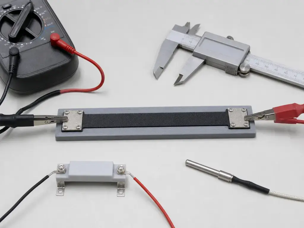
A two-terminal multimeter measurement captures the whole path, not just the conductive filament itself. That path includes the printed specimen, the leads, the probe tips, and the contact zones where current enters the part. When the sample is short or only moderately conductive, lead resistance and especially contact resistance can distort the number enough to make repeated measurements look inconsistent. A four-probe or four-wire setup is better for serious characterization, but a maker can still get useful comparative data if geometry, probe pressure, and contact method stay fixed. [11] [26]
Multi3D provides a good manufacturer example. Using its stated resistivity of 0.006 Ω·cm, a 10 cm length of 1.75 mm filament at 0.176 cm diameter works out to about 2.5 Ω, yet the same FAQ reports contact resistance of 0.5 Ω with silver paste and 2.4 Ω with screw terminals. [11] In other words, the contact method alone can rival the sample resistance.
Conductive PLA Filament Deep-Dive: Anisotropy, Print Parameters, and Apparent Resistivity
Conductive PLA is not isotropic, so one number rarely describes it well. The same product can measure differently as molded resin, along the printed roads, and across the layer stack. ProtoPasta’s technical page makes that clear. [8]
ProtoPasta reports 15 Ω·cm for molded resin, 30 Ω·cm for printed XY parts, and 115 Ω·cm for printed Z parts, all as manufacturer figures on its technical page. The same page also gives typical filament resistance of 2–3 kΩ per 10 cm for 1.75 mm filament and 800–1200 Ω per 10 cm for 2.85 mm filament. [8] That spread fits the basic structure of printed parts: current usually moves more easily along deposited roads than across interlayer interfaces and voids.
Apparent resistivity also shifts with how the part is printed and how it is measured. A 2026 study on ProtoPasta conductive PLA examined the influence of printing temperature, printing speed, and layer height on apparent resistivity, repeatability, and time-dependent drift over a 0–50 h interval. [20] A separate methods paper compared two-probe and four-probe measurements on ProtoPasta-based printed specimens and examined how electrode type and electrical bonding affect the reported resistivity. [26] In practice, extrusion temperature, infill, layer bonding, contact preparation, and probe layout can all move the number. Treat a conductive PLA value as a test result under stated conditions, not as a universal constant.
Types of Conductive 3D Printing Filament
Different conductive filament families are not directly rankable unless they are reported in the same metric and test context. A product page giving kΩ per 10 cm of raw filament is not directly comparable with a paper reporting Ω·cm for a printed trace, and neither is directly comparable with an ESD resistance window. The split below keeps circuit-oriented materials separate from ESD-oriented materials.
| Material/type | Metric + test context | Useful for | Main limitation |
|---|---|---|---|
| Carbon-black conductive PLA | 2.0–3.5 kΩ per 10 cm of 1.75 mm filament, or 0.7–1.3 kΩ per 10 cm of 2.85 mm filament, on the current ProtoPasta product page (Manufacturer; raw filament, not printed coupon). [9] | Simple low-current traces, touch pads, resistor-like elements | Printed resistance still depends on geometry, print direction, and settings. [8] |
| CNT PLA | 120 Ω·m at 210 °C, 103 Ω·m at 220 °C, and 97 Ω·m at 230 °C on 4 × 4 × 120 mm, 100% infill specimens at 10 V (Manufacturer). [13] | Sensors and conductive structures where process tuning matters | Slightly abrasive; hardened steel or ruby nozzle recommended. [13] |
| Low-resistance metal-polymer filament | 10,000 S/m and 1,000 S/m options on the Electrifi filament page (Manufacturer claim). [10] | Embedded contacts and lower-loss interconnect experiments | A manufacturer claim, not a universal wire replacement; contact method still matters. [10] [11] |
| PE-based conductive metal-polymer filament | ~0.012 Ω·cm volume resistivity and melting temperature up to 115 °C on Electrifi Conductive PE (Manufacturer). [12] | Conductive parts needing better heat tolerance than the base filament | The manufacturer says it adheres to PE and PP and is not compatible with PLA, ABS, or PETG. [12] |
| Research comparator: carbon black / graphene / copper | 12 Ω·cm, 0.78 Ω·cm, and 0.014 Ω·cm respectively in printed traces (Peer-reviewed; Flowers et al., 2017). [17] | Benchmarking and first-pass design estimates | Not a product ranking; geometry and print method still matter. [17] |
| Flexible conductive TPU | ~3.9 Ω·cm electrical resistivity with 245–250 °C nozzle, 50–60 °C bed, and 20 mm/s suggested print speed (Manufacturer TDS; Conductive Filaflex). [16] | Wearables and flexible sensing parts | Flexible, but still not a low-resistance wire substitute. [16] |
| Material/type | Metric + test context | Useful for | Main limitation |
|---|---|---|---|
| Spectrum PLA ESD | Surface resistivity 10^7–10^9 Ω/sq for printed parts on the product page (Manufacturer). [14] | Charge-control trays, covers, fixtures, and handling aids | Designed for ESD behavior, not low-resistance current carrying. [14] |
| 3DXTECH 3DXSTAT ESD-PLA | Target surface resistance 10^4–10^9 Ω on the product page (Manufacturer). [15] | ESD tooling and dissipative parts | A resistance window, not a wire-like conductor. [15] |
| ESDA classification context | Conductive below 1.0 × 10^4 Ω, dissipative from 1.0 × 10^4 Ω to below 1.0 × 10^11 Ω, insulative at or above 1.0 × 10^11 Ω for surface or volume resistance (Official documentation). [4] | Understanding what “ESD-safe” claims are trying to target | Low charging behavior is not guaranteed by resistance alone. [5] |
Buyer-Facing Decision Guide: Pick the Right Conductive Filament for the Job
The right conductive filament depends on the job, not on the loudest marketing line. Multi3D describes Electrifi as “the world’s most conductive 3D printing filament,” but that is a manufacturer claim, not a verified market-wide ranking. [10] Independent literature supports the idea that filler choice can change printed-trace resistivity by orders of magnitude, but it does not establish one universal winner across all products, geometries, and test methods. [17]
Use-case → material target:
- Capacitive touch pad → conductive PLA or another moderately conductive filament with repeatable geometry. [8] [9]
- Resistive sensor or flex sensor → conductive PLA or flexible conductive TPU where resistance change is part of the design. [16] [18]
- Low-current trace or jumper prototype → conductive filament only for educational, signal-level, or very low-load use. [17] [18]
- Embedded contact pads → higher-conductivity metal-polymer systems, checked with a controlled contact method. [10] [11]
- ESD fixture or tooling → ESD-oriented filament specified by resistance window and application context. [4] [14] [15]
- Use copper wire or PCB instead → when you need stable interconnects, lower resistance, tighter tolerances, or predictable current handling. [17]
No reliable market-wide most conductive filament figure was found in the available sources.
Worked Example: Estimating Trace Resistance Before You Print
If you want a first-pass estimate for conductive filament used in PCB-style traces, start with the geometry you actually intend to print. As an example only, take a straight trace with length L = 10 cm and cross-sectional area A = 1 mm². Flowers et al. reported printed-trace resistivities of 12 Ω·cm for a carbon-black filament and 0.014 Ω·cm for a copper-filled filament in a peer-reviewed comparison, which makes them useful inputs for a unit-safe estimate. [17]
Use (R = \rho L / A). Convert the source resistivities from Ω·cm to Ω·m by multiplying by 0.01, so 12 Ω·cm becomes 0.12 Ω·m and 0.014 Ω·cm becomes 0.00014 Ω·m. Convert the geometry to SI units as well: 10 cm = 0.1 m and 1 mm² = 1 × 10^-6 m². That gives (R = 0.12 × 0.1 / 1 × 10^{-6} \approx 12{,}000) Ω for the carbon-black case and (R = 0.00014 × 0.1 / 1 × 10^{-6} \approx 14) Ω for the copper-filled case. [17] The gap is the point: how conductive a filament feels in use depends as much on filler system and cross-section as on the spool label. This is a first-pass estimate, not a guaranteed part-performance claim.
Joule Heating & Current Testing
A printed trace that works at a multimeter’s tiny test current may still fail at the current you actually want to run. Power loss rises as I²R, so even a modest current can create useful heat or unwanted overheating when the trace resistance is high. In Flowers et al., example 10 cm traces could land around 150 Ω or 7500 Ω depending on the conductive filament being discussed, which is already enough to make current handling highly application-specific. [17]
Safety check: load-test at the intended current, start conservatively, and watch for temperature rise, softening, odor, discoloration, or layer separation. Conductive printed polymers can power simple circuits and sensors, but their resistivity is high enough that current testing belongs in the workflow, not as an afterthought. [17] [18]
Workflow: How to Print and Measure a Conductive Trace Coupon
Start with a straight coupon, not a decorative part. A simple bar or straight trace is easier to measure and compare across settings. Print it with the same nozzle, layer height, temperature, speed, and infill you plan to use in the real part, then measure the finished width, thickness, and length after cooling. If you think you may later compare bulk-like resistance with ESD-style planar behavior, keep the geometry simple and add consistent contact pads at both ends.
- Print a straight coupon with final settings.
- Measure dimensions after printing.
- Use a consistent contact or electrode method.
- Record temperature and humidity if relevant.
- Test current and heating at the intended load.
Measurement discipline matters as much as the print. Multi3D’s manufacturer example shows 0.5 Ω contact resistance with silver paste and 2.4 Ω with screw terminals, so changing the contact method can move the reading even if the printed sample is unchanged. [11]
This is a repeatable maker workflow, not a certification claim. For moderately conductive materials, ASTM D4496 is the best standards anchor, covering about 10^0 to 10^7 Ω·cm volume resistivity or 10^3 to 10^7 Ω per square surface resistivity at 23 °C and 50% RH. [3] ASTM D257 is still worth knowing, but ASTM explicitly says it is not suitable for moderately conductive materials and points users to D4496. [2] If the part is being evaluated as a planar ESD material rather than as a circuit trace, STM11.11-2022 is the surface-resistance context and STM11.12-2021 is the volume-resistance context. [6] [7]
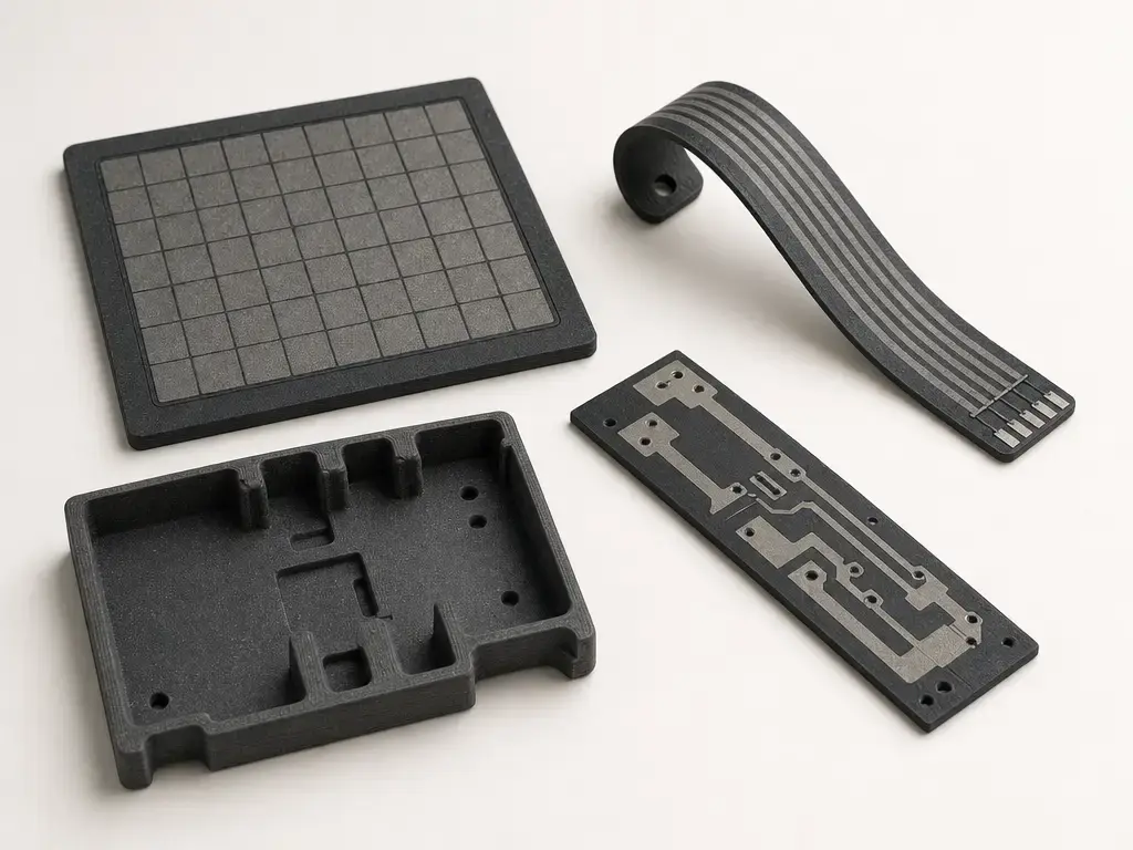
Applications: Sensors, Touch Pads, ESD Tools, and PCB Prototypes
Conductive filament is most useful when treated as a low-current, geometry-sensitive material rather than a metal substitute. That makes it suitable for capacitive touch pads, resistive sensors, flex sensors, embedded contacts, and educational circuits. A 2017 study by Kwok et al. reported practical circuits printed with filament at roughly 5 × 10^-3 Ω·m resistivity, powered from a 9 V battery, plus sunlight stability over one month and no observable resistance degradation during seven days at 12 V AC in the described tests. [18] Those results are encouraging, but they do not remove the basic constraint that ordinary printed geometries can still end up fairly resistive. Flowers et al. cited example estimates of about 150 Ω and 7500 Ω for 10 cm-long, 2 mm-thick traces from historical conductive filaments, which is why path length and cross-section dominate the design. [17]
That is the right way to read the phrase conductive filament for PCB: prototype, low-current, or educational use, not copper replacement. For ESD tools, trays, or handling fixtures, the goal is controlled charge behavior rather than signal conduction, and ESDA warns that low charging properties are not necessarily predicted by resistance or resistivity alone. [5] Circuit conduction and ESD protection are related but different design problems.
Limitations and Failure Modes
The first limitation is resistance. Conductive PLA can be usable, but it is often resistor-like rather than wire-like. ProtoPasta’s technical page gives 30 Ω·cm for printed XY parts and 115 Ω·cm for printed Z parts, both manufacturer figures, so orientation alone can shift performance by nearly a factor of four. [8] Contact resistance compounds the problem because a two-terminal reading may reflect the meter setup almost as much as the printed path. [11] At higher loads, Joule heating becomes another failure mode, especially in long or thin traces.
Environmental and lifecycle effects matter too. Multi3D reports an accelerated 85 °C / 85% RH test in which resistivity doubled after 24 h, which is a manufacturer result rather than an independent standard qualification. [11] Reprocessing can degrade conductivity as well: Cieślik et al. reported that after five reprocessing cycles, conductivity fell to 0.06 S/cm at 190 °C and 0.03 S/cm at 200 °C, described as 1.7× and 3.7× decreases. [19]
Material choice and hardware wear add more uncertainty. Spectrum’s electrically conductive PLA page recommends a hardened steel or ruby nozzle because the CNT-filled filament is slightly abrasive. [13] An academic 2023 study on nozzle wear used abrasive copper-reinforced filament to wear nozzles deliberately and found brass more prone to wear than steel, with the geometry change affecting subsequent PLA print accuracy. [24] Layer delamination is another practical electrical failure mode because interrupted interlayer contact raises resistance or breaks the path completely. Finally, headline numbers often disagree because different sources are not measuring the same thing: manufacturer filament-resistance figures, two-probe coupon readings, four-probe resistivity measurements, and ESD resistance windows are not interchangeable. [20] [26]
Current Research and Market Context
Conductive filament sits inside a broader additive-manufacturing field that includes electrically conductive polymers, polymer nanocomposites, and printed functional structures for sensing, electronics, and shielding. A 2022 review by Ryan et al. maps that wider landscape and its limitations, while studies such as Flowers et al. and Kwok et al. show why the field remains application-specific rather than plug-and-play. [21] [17] [18] In practice, the spread from carbon black to graphene to copper-filled systems is large enough that conductive filament is better understood as a design space than as a single performance class. [17] When the job needs lower resistance or higher repeatability, the alternatives are usually hybrid ones: embedded wires, copper tape, conductive inks, or conventional PCB assembly.
Choosing Conductive Filament: Practical Takeaways
Conductive filament is best chosen by function. The key question is not whether it conducts at all, but whether its measured resistance, geometry, and print direction fit the task. [8] [17]
Use conductive PLA when you want printable resistor-like behavior for low-current traces, touch pads, or sensors; the current ProtoPasta product page explicitly frames printed resistance as geometry- and settings-dependent and gives typical raw-filament resistance in the kΩ-per-10-cm range. [9] Use ESD-oriented filament when the goal is charge control inside conductive or dissipative resistance windows, not low-loss power delivery. [4] [5] Use higher-conductivity metal-polymer systems only with careful measurement discipline and realistic expectations. [10] [11] If the job needs a stable interconnect, predictable heating behavior, or low voltage drop, copper wire or a conventional PCB is usually the better choice. [17]
FAQ
What is conductive filament?
Conductive filament is a 3D-printing feedstock formulated so a printed part can pass current to some degree, bleed off charge, or act as a sensing element. In this article’s context, it is mainly used in material-extrusion printing and usually gets its behavior from fillers such as carbon black, carbon nanotubes, graphene-derived carbon, or metal-rich conductive systems. [1] [27]
How conductive is conductive filament compared with wire?
Usually much less conductive than wire. In one peer-reviewed printed-trace comparison, resistivity values were 12 Ω·cm for carbon black, 0.78 Ω·cm for graphene, and 0.014 Ω·cm for copper-filled filament, which is a huge spread but still far above metal-interconnect expectations in most real designs. [17]
Is conductive PLA filament good for PCB prototyping?
It can be useful for prototype, low-current, or educational work, which is the only safe way to read conductive filament for PCB claims. Conductive PLA can work for touch pads, sensor traces, and simple interconnect experiments, but printed resistance remains geometry-dependent and anisotropic, so it is not a drop-in substitute for copper PCB traces. [8] [17]
Is ESD conductive filament the same as electrically conductive filament?
No. ESD materials are selected for controlled charge behavior, not for wire-like conduction. ESDA’s material classes are based on resistance windows, with conductive below 1.0 × 10^4 Ω, dissipative from 1.0 × 10^4 Ω to below 1.0 × 10^11 Ω, and insulative at or above 1.0 × 10^11 Ω. [4]
How do I measure conductive filament with a multimeter without fooling myself?
Keep the coupon geometry and the contact method fixed. A two-terminal reading includes the sample, the leads, and the contact points, so changing from one contact style to another can shift the number significantly. Multi3D’s example reports 0.5 Ω with silver paste and 2.4 Ω with screw terminals. [11]
Expert: Why do two-probe and four-probe measurements disagree so much on conductive PLA?
Because two-probe measurements include lead and contact resistance, while four-probe measurements separate current delivery from voltage sensing and reduce those external errors. A 2024 ProtoPasta-based methods paper compared the two approaches and examined how electrode type and bonding technique changed the reported resistivity. [26] Multi3D’s contact-resistance example shows why this matters in practice. [11]
Expert: What resistance range is good enough for a printed trace, and how do I design around it?
There is no universal threshold. Start from current, path length, cross-section, and heating, then estimate resistance and verify it on a printed coupon. Peer-reviewed printed-trace data already span from 12 Ω·cm for carbon black to 0.014 Ω·cm for copper-filled material, and real trace resistance can still rise sharply with ordinary geometry. [17]
Sources
- ISO/ASTM 52900:2021 Additive manufacturing — General principles — Fundamentals and vocabulary
- ASTM D257 Standard Test Methods for DC Resistance or Conductance of Insulating Materials
- ASTM D4496 Standard Test Method for D-C Resistance or Conductance of Moderately Conductive Materials
- ESDA Fundamentals Part 1
- ESDA Fundamentals Part 3
- ANSI/ESD STM11.11-2022 table of contents PDF
- ANSI/ESD STM11.12-2021 table of contents PDF
- ProtoPasta Conductive PLA technical page
- ProtoPasta Conductive PLA product page
- Multi3D Electrifi product page
- Multi3D FAQs
- Multi3D Electrifi Conductive PE product page
- Spectrum PLA Electrically Conductive page
- Spectrum PLA ESD page
- 3DXTECH 3DXSTAT ESD-PLA page
- Recreus Conductive Filaflex technical data sheet
- Flowers et al. 2017, “3D printing electronic components and circuits with conductive thermoplastic filament”
- Kwok et al. 2017, “Electrically conductive filament for 3D-printed circuits and sensors”
- Cieślik et al. 2023, “Multiple Reprocessing of Conductive PLA 3D-Printing Filament”
- Polymers 2026, “Influence of 3D Printing Parameters on Apparent Resistivity, Repeatability and Time-Dependent Drift of Conductive PLA”
- Ryan et al. 2022 review on additive manufacturing of electrically conductive polymers and nanocomposites
- Keysight application note on sheet resistance and resistivity
- IUPAC Gold Book graphene layer entry PDF
- “Influence of the nozzle wear on 3D printing quality” study record
- “Effects of nozzle material and its lifespan on the quality of PLA parts manufactured by FFF 3D Printing”
- “On the Electrical Resistivity Measurement Methods and Properties of Conductive 3D-Printing PLA Filaments”
- ISO/ASTM 52903-1:2020 Additive manufacturing — Material extrusion-based additive manufacturing of plastic materials — Part 1: Feedstock materials