Summary
Electron Beam Melting (EBM) is an advanced metal 3D printing technology categorized within powder bed fusion techniques. Introduced commercially in 1997 by Arcam AB, Sweden, EBM employs a high-energy electron beam to selectively melt metal powder, layer by layer, in a vacuum environment. EBM offers exceptionally fast scan speeds but generally lower precision and rougher surface finish compared to Selective Laser Melting (SLM). Its applications are limited to a narrow range of metals due to process and material compatibility requirements, but its unique vacuum system makes it suitable for reactive alloys where SLM may struggle. [1][9][16]
Historical Background
The foundational patent for Electron Beam Melting was filed in 1993 by Swedish company Arcam AB in partnership with the Chalmers University of Technology, Gothenburg—a key milestone in industrializing high-energy additive manufacturing. [2]
Arcam AB was founded in 1997 by Ralf Larson and Jarl Assmundson in Sweden, marking the advent of commercial EBM systems. The company has since played a pivotal role in globalizing EBM technology. [8]
Technical Principles
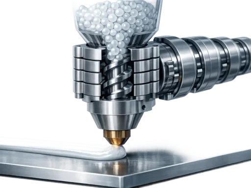
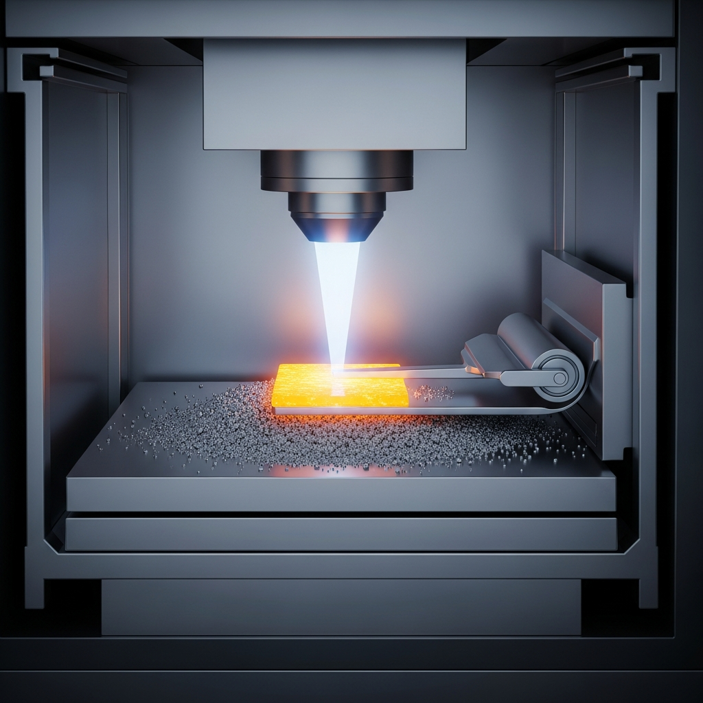
At its core, EBM is a powder bed fusion process performed in a vacuum chamber. An electron beam generated by a tungsten filament is focused and scanned across a bed of metal powder, melting selective regions to form each layer. The process operates at high build temperatures—typically between 700 and 1,000 °C—with initial preheat temperatures in the 650–1,000 °C range. Typical layer thicknesses sit between 50 and 200 μm, while beam currents range from approximately 5 to 40 mA. Scan speeds vary significantly, from 500 to 10,000 mm/s depending on system and application. The high ambient temperature minimizes thermal gradients, reducing residual stresses found in post-processed parts. [3][4][5][6][7]
Electron Beam Melting differs markedly from Selective Laser Melting, which uses a focused laser (photon-based) as its heat source rather than electrons. SLM systems operate in an inert gas—typically argon—environment, while EBM mandates a high vacuum to prevent electron scattering and oxidation. The vacuum environment also facilitates processing highly reactive or oxidation-prone alloys. Other critical distinctions include differences in powder spreading methods, thermal management strategies, and cooling rates, which collectively impact surface finish, accuracy, and material compatibility. [12]

| Parameter | EBM | SLM |
|---|---|---|
| Energy Source | Electron beam | Laser (photon) |
| Layer Thickness | 50–200 μm (typical: 70 μm) | 20–50 μm |
| Beam Power | Up to 4,500 W | Up to 1,000 W |
| Scan Speed | Up to 8,000 mm/s | Lower velocity (typically <2,000 mm/s) |
| Build Volume | Cylinder: Ø350 × 430 mm | 600 × 600 × 600 mm box |
| Build Environment | Vacuum | Inert gas (argon/nitrogen) |
| Residual Stresses | Very low | Medium |
| Surface Finish | Rougher | Smoother, higher precision |
Types and Variants
The term Selective Electron Beam Melting (SEBM) is often used synonymously with EBM. A related but distinct process is Electron Beam Freeform Fabrication (EBF³), developed at NASA in 1995 by Vivek Davé. While EBM is a powder-bed process, EBF³ deposits wire feedstock in a layer-by-layer manner for near-net-shape components, especially in space applications. [15]
Performance
EBM demonstrates a distinct speed advantage over other powder bed techniques—electron beam scan speeds can reach as high as 8,000 mm/s, enabling faster build times, especially for large or multiple-part builds. This speed contributes to notable throughput in industrial settings. [13]
With respect to accuracy and surface finish, EBM generally produces coarser results than SLM. Typical layer thickness for EBM is around 70 μm (with a practical range of 50–200 μm), while SLM often achieves finer layers between 20 and 50 μm. As a consequence, EBM parts tend to have rougher surfaces and less fine detail, making post-processing essential for components requiring tight tolerances or smooth surfaces. [9][16]
One of EBM’s defining advantages lies in its mechanical properties. The process’s high build temperature leads to very low residual stresses, minimizing the risk of warping or cracking post-build—an asset for high-integrity aerospace and medical implants. The environment is especially advantageous for processing reactive alloys, such as Ti‑6Al‑4V, Inconel 718, and CoCrMo, which are difficult to handle in oxygen-rich or argon-based environments. However, EBM’s material range remains much more restricted than SLM, with most implementations mature only for several titanium alloys and select superalloys. Typical EBM parts achieve densities exceeding 99.5%, but parameters such as beam current, layer thickness, and scan speed must be precisely controlled to minimize internal porosity and achieve consistent quality. [14][15][3]

Applications
EBM’s unique thermal profile and low-residual-stress process make it popular in industries with demanding material and mechanical requirements. In aerospace, EBM is used to produce lightweight, structurally optimized engine components and brackets where reliability and strength are paramount. The medical sector relies on EBM for producing orthopedic implants—particularly made from Ti‑6Al‑4V—where bone integration and mechanical strength are critical. The automotive sector utilizes EBM for prototypes and high-stress drivetrain parts. Nonetheless, parts often require post-processing due to their relatively rough surfaces and high initial cost of machinery and powders. [14][15][16]
Key application areas include:
- Aerospace turbine blades, brackets, and structural components
- Custom medical implants (e.g., orthopedic, dental)
- Prototyping and small-batch automotive parts
- Research on heat exchangers and lattice structures for weight reduction
Research Updates
Recent research on EBM focuses on expanding the suite of compatible alloys, particularly aiming to enable reliable processing of aluminum and copper—both challenging due to high reflectivity or high thermal conductivity. Advances in electron beam stability, adaptive preheat strategies, and closed-loop monitoring systems are designed to improve surface quality and minimize internal defects. Efforts are ongoing to optimize beam parameters and powder characteristics for better accuracy, denser builds, and reduced post-process requirements. Materials development remains a principal challenge, as does maintaining quality assurance for thin-walled or low-density geometries. [16]
Q&A (FAQ)
1. What is Electron Beam Melting in metal 3D printing?
Electron Beam Melting (EBM) is a metal 3D printing technique where a high-energy electron beam selectively melts layers of metal powder in a vacuum to build dense, near-net-shape parts. [1]
2. How does EBM differ from SLM regarding accuracy and speed?
EBM achieves higher scan speeds—up to 8,000 mm/s—compared to SLM but typically offers lower accuracy and produces rougher surfaces, with layer heights of 70 μm versus SLM’s 20–50 μm range. [9][13]
3. Why does EBM require a vacuum environment?
EBM requires a vacuum to keep electrons focused, minimize contamination, and enable processing of reactive alloys. Unlike SLM, which only needs inert gas, EBM’s electrons scatter in air and cannot function efficiently otherwise. [12]
4. Which materials are compatible with EBM?
EBM is commercially proven mainly with Ti‑6Al‑4V, Inconel 718, and CoCrMo alloys. Its material range is narrower than SLM due to vacuum system and powder requirements. [14]
5. What advantages does EBM offer for aerospace and medical applications?
EBM minimizes residual stresses thanks to its high build temperatures, allowing the manufacture of high-integrity, complex components suitable for implants and flight-critical aerospace structures. [15]
6. Expert-level: What are the main challenges in using EBM for aluminum alloy parts?
Aluminum presents challenges in EBM due to its high reflectivity, rapid heat dissipation, and tendency for powder bed instabilities, making processing difficult and research ongoing. [16]
7. Expert-level: What parameters (beam current, scan speed, layer thickness) most influence part density in EBM?
Part density is mainly influenced by beam current (5–40 mA), scan speed (500–10,000 mm/s), layer thickness (50–200 μm), and build temperature (650–1,000 °C), which together determine melt quality and porosity levels. [4][5][6][7]
Sources
- Electron-beam additive manufacturing — Wikipedia
- What is electron beam melting? — TWI Global
- Electron beam melting — Italian Wikipedia
- Overview of electron beam melting technology — MET3DP
- Overview of electron beam melting technology — MET3DP
- Overview of electron beam melting technology — MET3DP
- Overview of electron beam melting technology — MET3DP
- Arcam — Wikipedia
- EBM vs. SLM 3D Printing — Xometry
- EBM vs. SLM 3D Printing — Xometry
- EBM vs. SLM 3D Printing — Xometry
- EBM vs. SLM 3D Printing — Xometry
- EBM vs. SLM 3D Printing — Xometry
- EBM vs. SLM 3D Printing — Xometry
- EBM residual stress — HNTIJO
- EBM limitations and research — HNTIJO